Applications:
|
|||||||||||||||||||||||||||||||||||||||||||||||||||||
Features:
|
|||||||||||||||||||||||||||||||||||||||||||||||||||||
Description:The PRL-8216 is a 2 x 1:8 DC coupled signal router designed for 50 Ω I/O applications. The usable frequency band extends from DC to >2.5 GHz. A signal connected to each input D can be routed to output Q1-Q8 in the same bank. It can also be used as a Reflective Scanner in the reverse direction to scan signals on the Q inputs at the D output. Because signals connected to the non-selected ports are not terminated, these signals will be reflected, hence the term reflective scanner. There are three related models:
The PRL-8108 is designed for scanning or routing single-ended signals, while the PRL-8216 can be used for simultaneous scanning or routing of differential signals. The PRL-8324 adds a third signal path for routing an additional signal, such as a timing reference. Each channel set is fully independent and can be controlled separately or slaved to another set's control input or switch, as described below. Each 8-channel bank has an 8-position rotary switch for manual channel selection, a toggle switch for Manual/Remote selection, and 8 LEDs for channel ID. Each set also has 3 x 2 stick pins (pulled up to +5V via 4.99 kΩ resistors) for TTL/CMOS remote control inputs. An parallel set of 3 x 2 stick pins allows control signals to be cascaded to additional sets or units for simultaneous switching. When the toggle switch is set to the Remote position (Up) the logic inputs are left open, Bits A0, A1, and A2 all float high, and channel Q8 is selected. Jumpers or remote inputs may be used to pull the pins low. When the unit is not powered, Q8 is also selected The pin designations and truth tables for the logic inputs are shown in Table I, and a block diagram is shown in Fig. 1. When the toggle switch is in the Manual (Down) position the rotary switch selects the channel, and the remote control pins should be disconnected.
Table I: Logic Input Truth table for PRL-8216 (each bank)
|
|||||||||||||||||||||||||||||||||||||||||||||||||||||
| Item | Description |
|---|---|
| PRL-8108-SMA | 1:8 Signal Router/8:1 Reflective Scanner, SMA I/Os |
| PRL-8216-SMA | 2 x 1:8 Signal Router/8:1 Reflective Scanner, SMA I/Os |
| PRL-8324-SMA | 3 x 1:8 Signal Router/8:1 Reflective Scanner, SMA I/Os |
| 88004001-0.33 | Cable, twisted pair, 1 x 2 header connectors, 4" length |
| 88004001-1 | Cable, twisted pair, 1 x 2 header connectors, 1' length |
| 88004001-6 | Cable, twisted pair, 1 x 2 header connectors, 6' length |
| 88003002-18 | Cable, 50 Ohm, SMA-M/SMA-M, 18" +/-0.1" tolerance |

A block diagram of a PRL-8108 PCB is shown above
- The PRL-8108 consists of one PCB
- The PRL-8216 consists of two identical PCBs in one enclosure. Each board operates independently unless the control pins are tied together via external cabling.
- The PRL-8324 consists of three identical PCBs.

Fig. 2: PRL-8216 Rear View
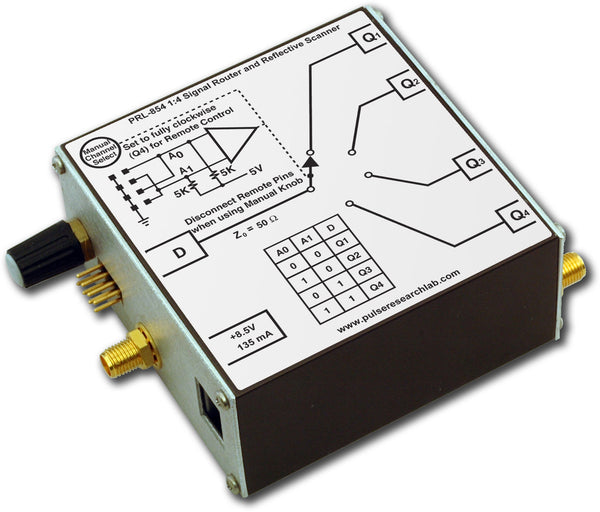
The PRL-854 series is well suited to cascading, in either direction, for creating configurations with larger channel counts and/or special applications, with no engineering required. Please see this Application Note where our sister company designed a set of PRL-854 and PRL-854DC units into a low-noise, high-speed, flexible test multiplexer:
SPECIFICATIONS (0° C ≤ TA ≤ 35° C)*
| SYMBOL | PARAMETER | Min | Typ | Max | UNIT | Comments |
|---|---|---|---|---|---|---|
| tr/tf | Rise/Fall Times (10%-90%) | 200 | 230 | ps | ||
| BW | Equivalent 3 dB bandwidth | 1.50 | 1.75 | GHz | ||
| RIN(RM) | Input Resistance, Logic inputs | 4.99 | kΩ | Pulled up to +5V | ||
| VIH | Logic Input Hi Level | 2.0 | 2.0 | 5.0 | V | |
| VIL | Logic Input Lo Level | -0.5 | 0.0 | 0.5 | V | |
| VSWR1 | VSWR, 25 MHz ≤ f ≤ 1.25 GHz | 1.35:1 | ||||
| VSWR2 | VSWR,1.25 GHz < f ≤ 2.4 GHz | 2.00:1 | ||||
| VO/VIN1 | Insertion Loss, selected Channel | 1.65 | 2.50 | dB | 625 MHz ≤ f ≤ 1.25 GHz | |
| VO/VIN2 | Insertion Loss, selected Channel | 6.00 | 10.00 | dB | 1.25GHz ≤ f ≤ 2.4GHz | |
| VO/VIN3 | Isolation, un-selected Channels | 40 | 46 | dB | 625 MHz ≤ f ≤ 1.25 GHz | |
| VO/VIN4 | Isolation, un-selected Channels | 32 | 38 | dB | 1.25 GHz ≤ f ≤ 2.4 GHz | |
| tPLH | Propagation Delay to Output ↑ | 900 | 1200 | ps | ||
| tSKEW | Skew between any 2 Outputs | 10 | 35 | ps | ||
| VINMAX | Maximum Input Voltage | 30 | V | |||
| IMAX | Maximum Switching Current | 0.5 | A | |||
| Switch Time | 6 | ms | ||||
| Expected Life Cycles | >106 | |||||
| VDC | DC Input Voltage | 7.5 | 8.5 | 12 | V | |
| IDC | DC Input Current | 660 | 720 | mA | ||
| VAC1 | AC/DC Adapter Input Voltage, 120 | 108 | 115 | 127 | V | |
| VAC2 | AC/DC Adapter Input Voltage, 220 | 216 | 230 | 254 | V | |
| Logic input for Remote operation, each bank | 3 x 2 pins (A0, A1, A2) | See Table I | ||||
| Size | 3.0 x 6.8 x 4.0 | in. | ||||
| Weight | 3 | lbs | Excluding AC adapter | |||
| Shipping Weight | 7 | lbs | Including AC adapter | |||


