Applications:
|
|
Features:
|
|
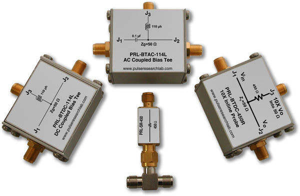
DescriptionPRL offers a series of AC-coupled and DC-coupled 50 Ω Bias Tees. There are three related models:
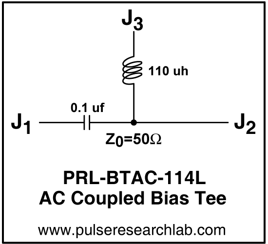
These devices enable insertion of a DC or low-frequency signal into a broadband 50 Ω coaxial transmission line system, while preserving the integrity of the high frequency characteristics of the 50 Ω I/O ports. Typical applications of Bias Tees include supplying DC bias to semiconductor devices, such as diode detectors, laser diodes, FETs and amplifiers, etc., housed in coaxial structures. In addition, the DC-coupled versions can provide DC offset to ground-referenced signals. Furthermore, the PRL-BTDC-450R is also a wide-band Inline 10X signal pick-off device which allows extraction of a small portion of the signal for monitoring, while producing negligible amount of disturbance to the main signal path. Each model has RF I/O ports, J1 and J2, and a Bias port, J3. The RF I/O path is a 50 Ω transmission line, either AC- or DC-coupled between the I/O connectors J1 and J2. The Bias port J3 is used for connecting a DC voltage, a constant current, or a low frequency signal source to the 50 Ω transmission line, while inductor L isolates the 50 Ω transmission line from the bias source. In the case of the PRL-BTDC-450R, J3 is connected to the I/O line through a 450 Ω resistor, which must be terminated into a 50 Ω input instrument for monitoring purposes. When so terminated the loading on the I/O line is 500 Ω. Since the I/O line looks like a 25 Ω load to the 450 Ω resistor, the signal loss due to the 500 Ω loading is only 5%. Traditional Bias Tees are AC coupled, as shown in Model PRL-BTAC-114L, where the RF signal is AC-coupled to the DUT, connected to J2 through coupling capacitor C. In many of today's digital applications, where signals with very long 1s and 0s are common, DC coupling is desirable, because it eliminates DC level shift due to duty cycle variations. Furthermore, when a constant current source is connected to the bias port, the lower 3 dB bandwidth can be extended to DC. The upper bandwidth of a Bias Tee is limited mostly by the imperfection of the isolation inductor L between the 50 Ω transmission line and the bias source. L is usually made up of different combinations of Ls and Rs. For the PRL series of Bias Tees, the upper 3 dB bandwidth is typically greater than 6 GHz. For the AC-coupled Bias Tee, the lower 3 dB bandwidth is determined by the dominant pole made up either by 2Z0C or 2L/Z0, assuming that both I/O ports are terminated into Z0 and that L is connected to a voltage source. For the DC-coupled Bias Tee, however, the lower 3 dB bandwidth is determined by L, and it can be extended to DC by using a constant current instead of a voltage bias source. Standard value for the coupling capacitor C is 0.1 µf and the isolation inductor L is 110 µh. Other values are available by special order. When used with the PRL series of Coupling and Termination modules the lower 3 dB bandwidth of the DC-coupled model can be customized by using different DC blocks, from 0.01 µf to 2.2 µf, and/or series-coupled inductors, up to 330 µh. Other components, such as feed-through decoupling capacitors or attenuators, also are available. |

PRL-BTAC-114L Block Diagram
SPECIFICATIONS (0° C ≤ TA ≤ 35° C)*
| SYMBOL | PARAMETER | Min | Typ | Max | UNIT | Comments |
|---|---|---|---|---|---|---|
| Z0 | I/O Line Characteristic Impedance | 48.5 | 50 | 51.5 | Ω | |
| IDC1 | J3 Bias Input Current | 300 | mA | L Input | ||
| VDC | J3 Bias Input Voltage | Limited by IDC | V | |||
| C | Coupling Capacitor | 0.08 | 0.10 | 0.12 | µf | |
| L | DC Bias Inductor | 110 | µh | |||
| RL | Inductor DC Resistance | 6 | Ω | |||
| TPLH/TPHL | Propagation Delay from J1 to J2 | 250 | 300 | ps | ||
| tr/tf | Rise/Fall Times (10%-90%) | 58 | 65 | ps | J1-J2 | |
| UBW | Equivalent Upper 3 dB Bandwidth | 5.3 | 6.0 | GHz | J1-J2 | |
| LBWC | Equivalent Lower 3 dB Bandwidth | 15.9* | KHz | |||
| Size | 1.0 x 1.3 x 1.5 | in | ||||
| Weight | 3 | Oz | ||||
*Limited by C
**Limited by L


